
Why AI Interconnects Are Moving from Wide & Slow to Narrow & Fast
Understanding the architectural shift behind next-generation AI systems

Understanding the architectural shift behind next-generation AI systems
The Bandwidth Dilemma
Optics form the backbone of long-range, high-speed communication, but transmission speed is fundamentally constrained by the physics of the optical component itself. Unlike electrical signals generated by SerDes circuits, the speed of an optical component is limited by its modulation bandwidth. Even when the driver provides a high-speed signal (e.g., 100 Gbps PAM4), the optical device itself often becomes the bottleneck.
Currently, optical components capable of direct modulation at 200G are extremely limited and costly. These typically require 200G VCSELs or Continuous Wave (CW) lasers paired with 200G silicon photonic modulators. To optimize production cost and power efficiency in server systems, the industry is now splitting into two distinct architectural philosophies to reach the next milestone of 3.2 Tbps per engine.
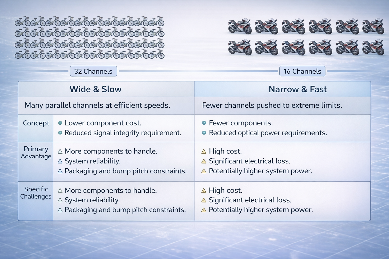
1. Narrow & Fast (The Current Bottleneck)
This approach uses fewer channels (e.g., 16 lanes × 200G) and pushes each lane to extreme physical limits in order to reduce fiber count. While this is technically feasible, it comes with a heavy “tax”:
- Signal Distortion: As data rates increase, signal integrity degrades rapidly.
- Power Penalty: To compensate for this distortion, power-hungry Digital Signal Processing (DSP) chips are required to recover the signal, significantly increasing overall system power consumption.
2. Wide & Slow (RVi’s XmartLink™ Solution)
This approach relies on massive parallelism, using a large number of channels (e.g., 64 lanes × 50G) operating at more efficient speeds. Although this increases the number of optical devices, eliminating complex signal compensation ICs (DSPs) results in substantial power savings.
The main challenge lies in integration. Packing a high density of optical devices and fibers into a limited space is mechanically difficult. RVi’s XmartLink™ overcomes this physical density barrier through proprietary Micro-VCSEL technology and advanced packaging solutions.
- Micro-VCSEL: A discrete VCSEL chip with a footprint five times smaller than standard VCSEL devices. This enables much higher component density and overall bandwidth density, meeting the demands of next-generation AI data centers.
- RVi Proprietary Advanced Packaging (RPAP): Conventional packaging technologies struggle with chips smaller than 100 μm, where placement, bonding, and repair become extremely challenging. RVi’s RPAP delivers a full-stack solution for handling micro-sized chips down to 5 μm, covering transfer, precise placement, inspection, bonding, and repair.
By addressing both geometry and packaging challenges, RVi unlocks the superior physics of the “Wide & Slow” architecture for the 3.2T era.
